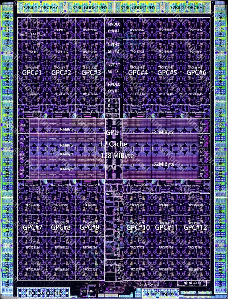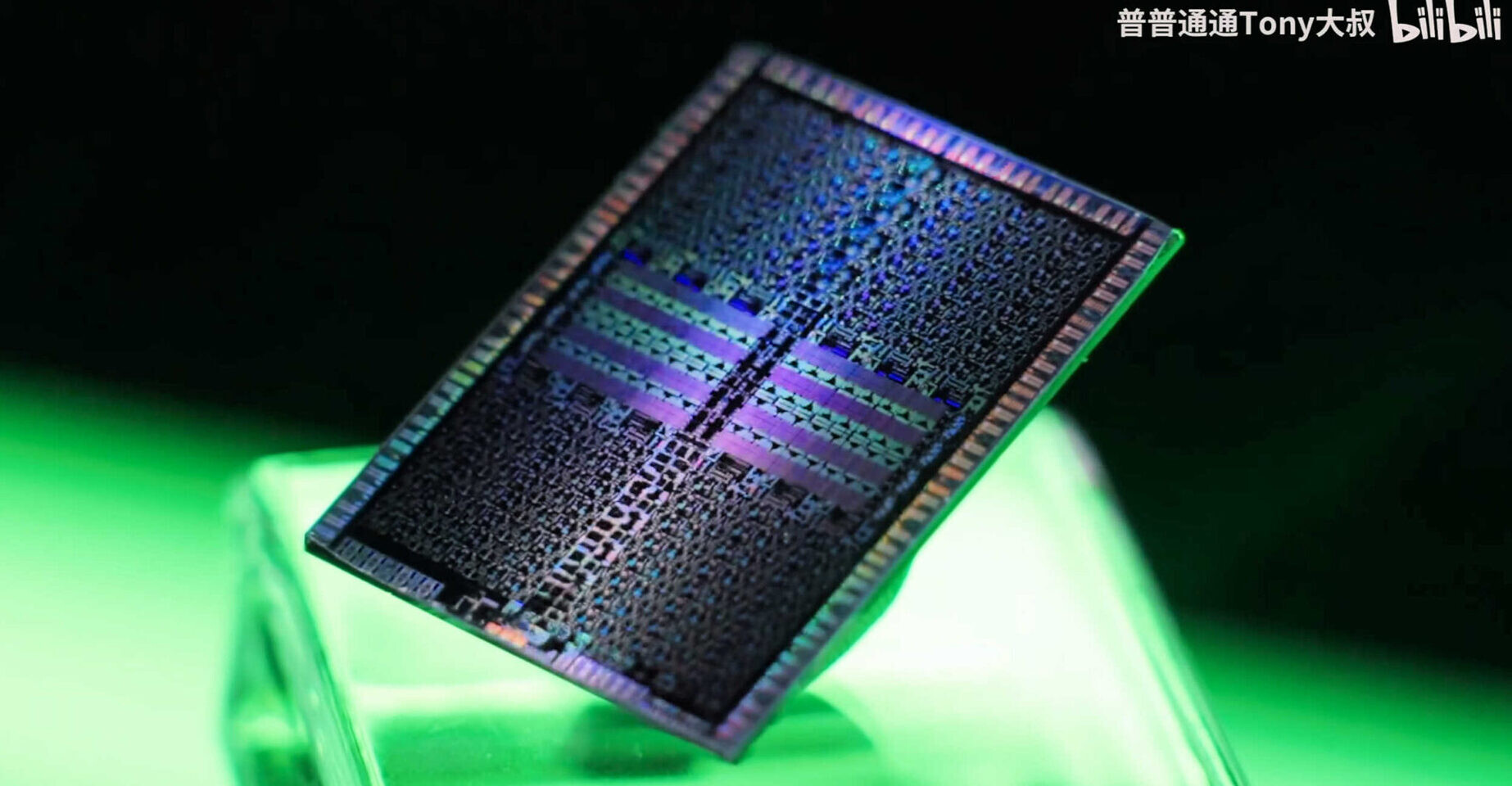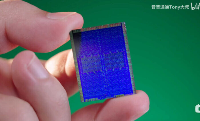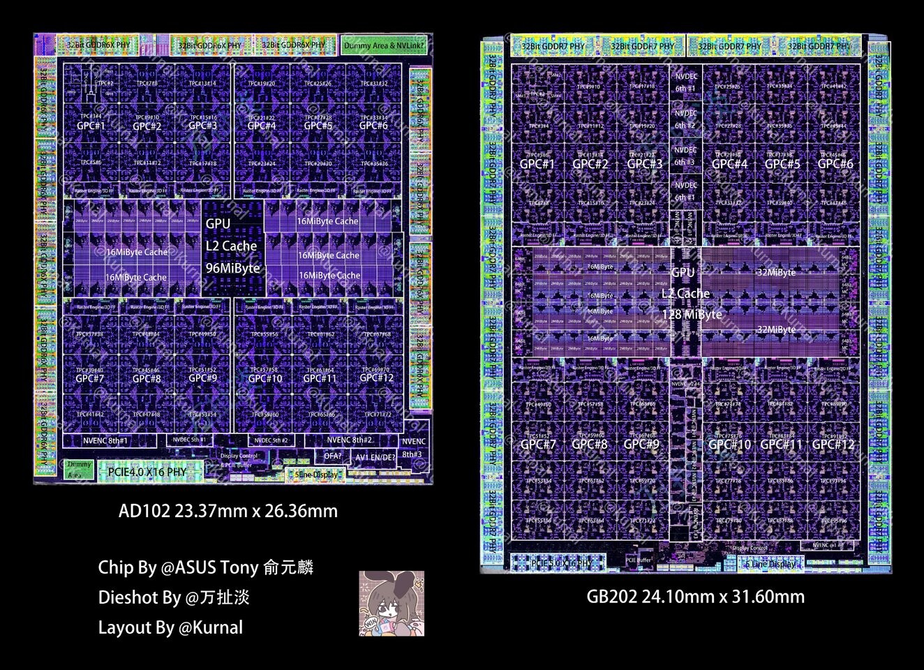
A recent die-shot of NVIDIA's GB202, the chip that powers the RTX 5090, has been revealed online, offering a detailed look at the physical layout of the "Blackwell" architecture. The annotated pictures, shared by hardware analyst Kurnal and provided by ASUS China general manager Tony Yu, compare the GB202 to its predecessor, the AD102, and highlight important architectural elements. The central area of the die contains 128 MB of L2 cache (96 MB enabled on the RTX 5090), surrounded by memory interfaces. There are eight 64-bit memory controllers that support the 512-bit GDDR7 interface, with physical interfaces located along the top, left, and right edges of the die. Twelve graphics processing clusters (GPCs) encircle the central cache. Each GPC consists of eight texture processing clusters (TPCs), with each GPC containing 16 streaming multiprocessors (SMs). The complete die setup allows for 24,576 CUDA cores, with 128 cores per SM across 192 SMs. The RTX 5090 has 21,760 CUDA cores, indicating that the full GB202 die is reserved for workstation GPUs.
The SM design features four slices that share 128 KB of L1 cache and four texture mapping units (TMUs). Each SM slice includes dedicated register files, L0 instruction caches, warp schedulers, load-store units, and special function units. A vertical strip in the die's layout houses the media processing components—NVENC and NVDEC units—that run from top to bottom. The RTX 5090 implementation supports three out of four available NVENC encoders and two out of four NVDEC decoders. There are twelve raster engine/3D FF blocks for geometry processing. At the bottom edge of the die are the PCIe 5.0 x16 interface and display controller components. Despite its size, the GB202 is smaller than NVIDIA's previous GH100 and GV100 dies, which were over 814 mm². Each SM includes specialized hardware, such as the new 5th-generation Tensor cores and 4th-generation RT cores, contributing to a total of 192 RT cores, 768 Tensor cores, and 768 texture units.