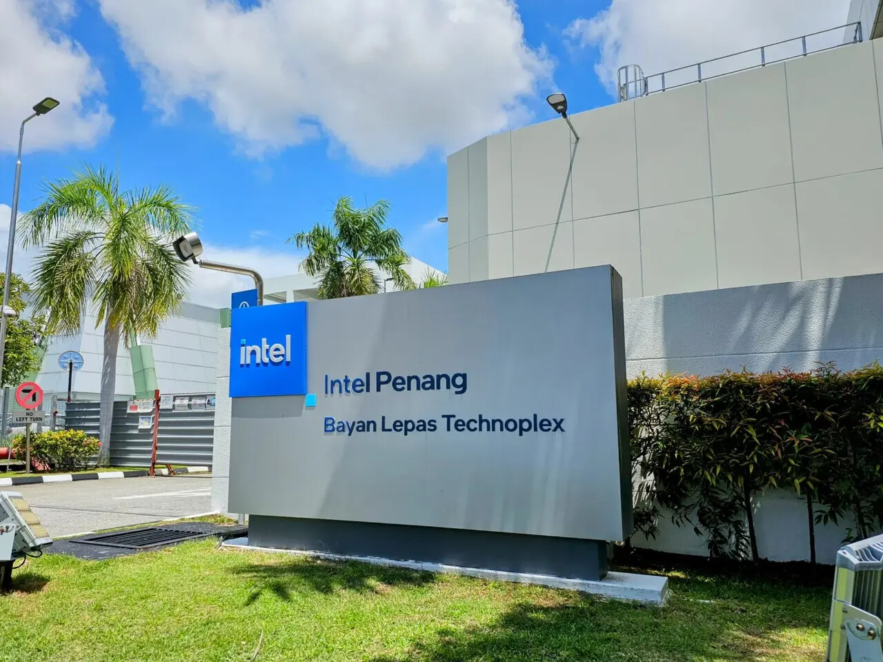
Intel Nears Completion of Advanced Packaging Facility in Malaysia
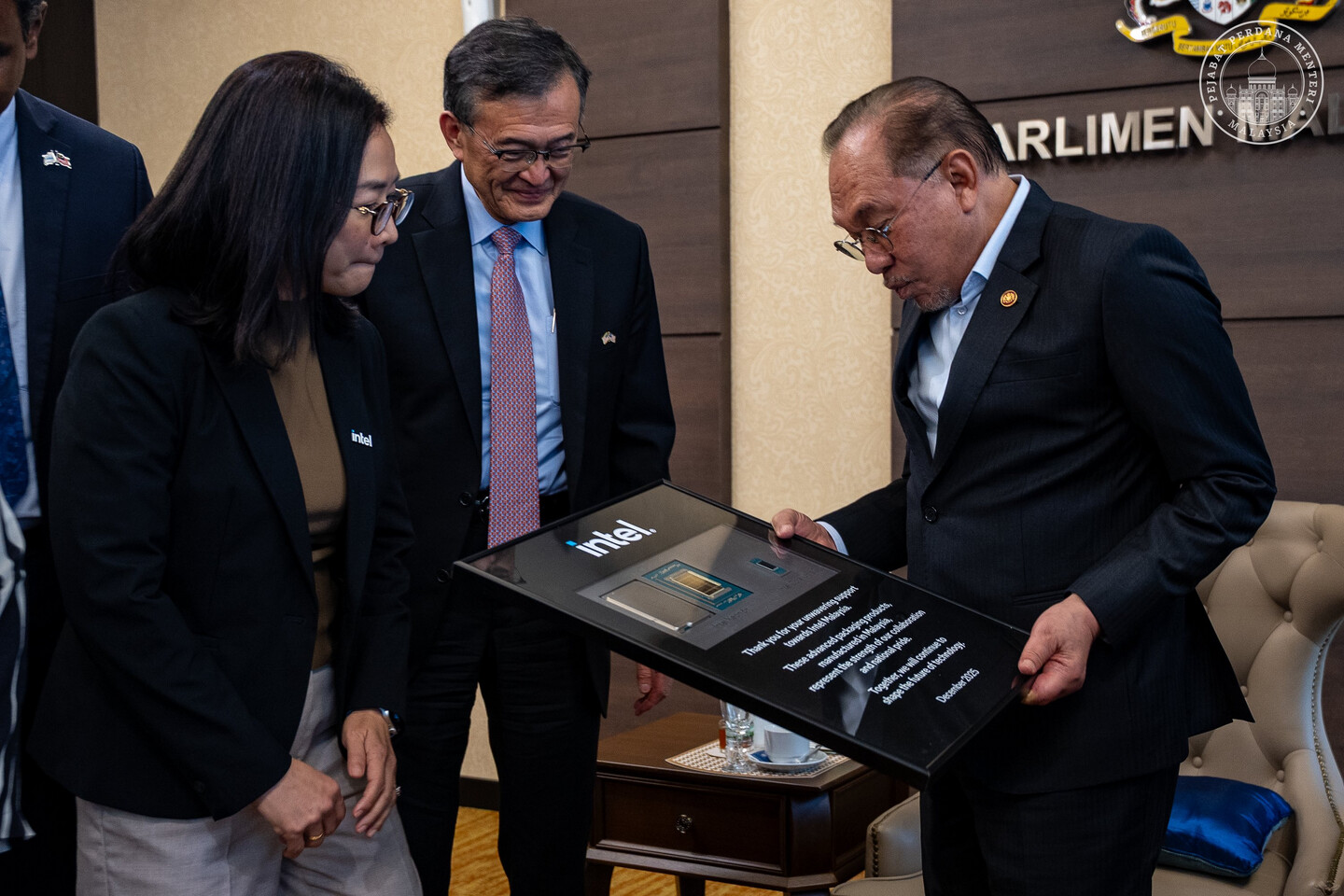
Intel is making significant strides in advanced semiconductor packaging with the near-completion of its new facility in Malaysia. According to reports from The Edge Malaysia, the complex—part of Intel’s Project Pelican—is now 99% finished and is expected to be fully operational later this year. Malaysian Prime Minister Datuk Seri Anwar Ibrahim recently met with Intel CEO Tan Lip-Bu and other executives to review the progress, underscoring the project's importance to both Intel and the region.
Project Pelican: A Key Step in Intel’s Foundry Expansion
The first phase of the Malaysian facility will introduce advanced assembly and testing capabilities, supporting Intel’s broader foundry expansion strategy. The site is engineered to manage die sorting, preparation, and full production flows for both EMIB (Embedded Multi-die Interconnect Bridge) and Foveros technologies. These advanced packaging methods are essential for high-volume, chiplet-based semiconductor designs, which are increasingly in demand for applications such as artificial intelligence and high-performance computing.
Intel has invested approximately $7 billion in Project Pelican, aiming to establish Malaysia as a central hub for its advanced packaging operations in the region. An additional $200 million has been allocated to complete the site, reflecting Intel’s commitment to scaling its manufacturing capabilities and supporting global semiconductor supply chains.
Advancements in EMIB and High-Bandwidth Memory Integration
Intel continues to refine its EMIB packaging technology, which differs from traditional silicon interposers used by competitors like NVIDIA. EMIB embeds conductive bridges directly into the substrate, offering a more cost-effective and efficient solution for high-density chips. This innovation enables Intel to scale up package sizes, moving from the current 100 x 100 mm to 120 x 120 mm, with plans for even larger 120 x 180 mm packages by 2028.
These larger packages are designed to support up to twelve HBM (High Bandwidth Memory) stacks, compared to eight in existing designs. Future iterations could accommodate as many as twenty-four HBM stacks, meeting the growing bandwidth and integration demands of AI and data center applications. Intel has also enhanced its EMIB-T technology, which now incorporates through-silicon vias (TSV) to support next-generation HBM4 memory. This advancement is entering mass production, positioning Intel to address the evolving needs of AI chipmakers.
Manufacturing Challenges and Industry Impact
While scaling up package sizes offers significant performance benefits, it also introduces new manufacturing challenges. Larger semiconductor packages are more susceptible to warpage and yield issues during production. Intel’s ongoing investments in advanced packaging technologies and manufacturing processes are aimed at overcoming these hurdles, ensuring reliable, high-volume output for next-generation chips.
With the near-completion of its Malaysian facility and continued innovation in packaging technologies, Intel is reinforcing its leadership in the global semiconductor industry and supporting the next wave of high-performance, chiplet-based designs.