Samsung Advances Toward 1000-Layer NAND Flash Storage
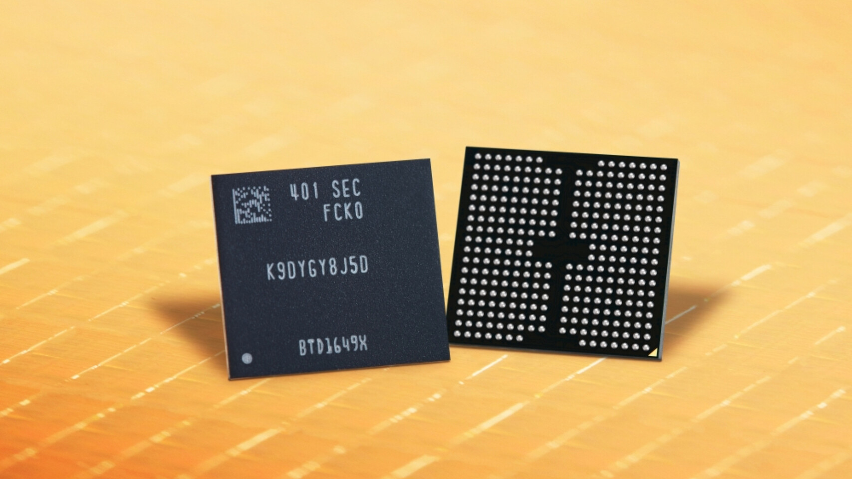
Samsung is making significant strides in the development of ultra-high-density NAND Flash storage, moving closer to its ambitious goal of 1000-layer V-NAND chips. As the complexity of manufacturing increases with each additional layer, Samsung is leveraging advanced packaging technologies rather than relying on a single chip solution. The company’s latest breakthrough involves stacking two 450-layer V-NAND modules to create a single 900-layer V-NAND chip, marking a major milestone in flash memory innovation.
Innovative Cell Multi-Bonding (CMB) Technology
According to a report from ET News, Samsung is utilizing Cell Multi-Bonding (CMB) technology, a sophisticated form of wafer stacking achieved through hybrid bonding. This process permanently fuses two silicon chips using embedded metal bumps, effectively creating a unified chip. Unlike traditional die stacking, Samsung’s approach connects entire silicon wafers by bonding their back ends together. This proprietary CMB process is a crucial step toward achieving 1000-layer V-NAND chips by 2030.
Overcoming Manufacturing Challenges
Samsung first introduced its 10th-generation V-NAND technology last year, which enabled the production of modules with over 400 layers. The company also debuted hybrid bonding at that time, and has since refined the technology to address new challenges. One significant hurdle is wafer warping, which becomes more pronounced with thicker 450-layer designs. To counter this, Samsung developed microscopic chucks and advanced bonding techniques to correct overlay and misalignment issues during the bonding process.
Within the NAND architecture itself, Samsung engineered new bitline and wordline structures to optimize power consumption and maintain manageable chip sizes. These innovations are essential for ensuring the reliability and efficiency of high-layer-count NAND chips.
Production Timeline and Industry Competition
While Samsung’s 900-layer V-NAND chip represents a major technological achievement, global availability is still on the horizon as high-volume production is expected to begin in the coming quarters. The immediate focus is on ramping up mass production of the 10th-generation V-NAND, which features over 400 layers per chip. The bonded 900-layer design will follow as manufacturing processes mature.
Currently, SK hynix holds the industry record for the highest number of layers in volume production with its 321-layer 4D NAND design. However, Samsung is poised to surpass this benchmark and set a new standard in NAND Flash storage density. Further updates from Samsung are anticipated as the company continues to push the boundaries of memory technology.